A New Semiconductor Could Transform Industries
A New Semiconductor Could Transform Industries
A new semiconductor greatly improves conduction to improve efficiency of high-temperature, high-powered applications.
By finding the right dopant, lowering the heat during synthesis, and doing the opposite of what everybody else has done for almost a century, engineers have turned a common electrical insulator into an ultra-wide bandgap semiconductor, a goal many researchers tried to reach over the years but failed to achieve.
For 80 years aluminum nitride (AlN) has been the working stiff of the electronics industry, serving as a reliable insulator and thermal conductor that’s excellent at quickly dissipating heat and maintaining efficiency in semiconductors. But Georgia Tech engineers have finally found a way to transform the staid insulator into p-type and n-type―the positive and negative charges electrical devices need to operate―ultra-wide bandgap (UWBG) semiconductors that could revolutionize several industries.
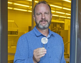
“Previously, you put AlN under the silicon chip or another material in a device to spread the heat,” said Alan Doolittle, Joseph M. Pettit professor in the school for electrical and computer engineering at Georgia Tech. “Now it is the device. It carries the current and does the switching while it carries the heat away.”
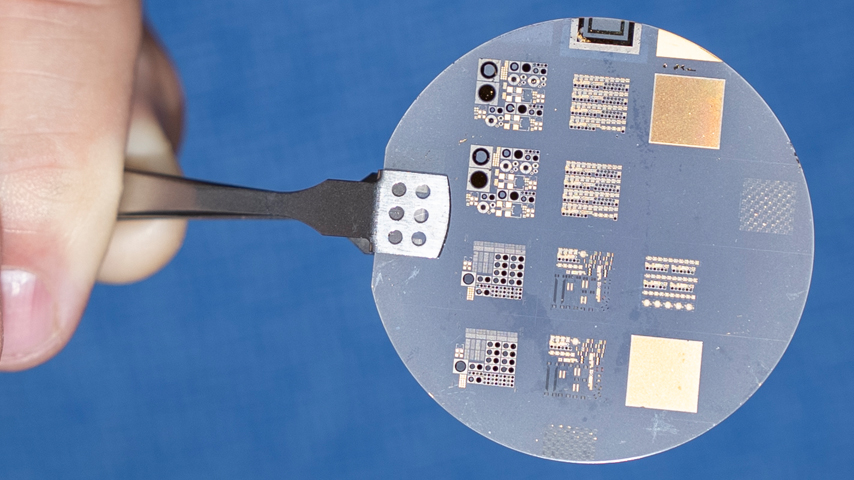
 Georgia Tech's Doolittle succeeds in converting an insulator into an ultra-wide bandgap semiconductor. Credit: Georgia Tech
Doolittle’s new AlN p-type semiconductor improves current conduction by 300 million times over exiting UWBGs, while the n-type improves it by 6,000 times, according to the research. That means they can be used, in many cases for the first time, to improve the performance and efficiency of high-powered, high-temperature applications such as high-voltage electronics, sensors, optoelectronics, deep ultraviolet LEDs for water purification and sterilization, biological warfare neutralization, solar blind detection for threat detection, utility grids for better control of power transmission, automated welding, and industrial laser cutting.
Georgia Tech's Doolittle succeeds in converting an insulator into an ultra-wide bandgap semiconductor. Credit: Georgia Tech
Doolittle’s new AlN p-type semiconductor improves current conduction by 300 million times over exiting UWBGs, while the n-type improves it by 6,000 times, according to the research. That means they can be used, in many cases for the first time, to improve the performance and efficiency of high-powered, high-temperature applications such as high-voltage electronics, sensors, optoelectronics, deep ultraviolet LEDs for water purification and sterilization, biological warfare neutralization, solar blind detection for threat detection, utility grids for better control of power transmission, automated welding, and industrial laser cutting.
“It opens up device opportunities that no one has ever even thought possible,” Doolittle said.
To make that happen, the material must have a high energy bandgap. Considered one of the most important properties of a semiconductor, the bandgap is the minimal amount of energy needed for electrical conduction. It also determines the voltage at which a device fails, also called breakdown. On top of that, bandgap represents the energy or wavelength of light that emanates from the semiconductor.
Become a Member: How to Join ASME
“Bandgap is the energy required to rip an electron off the molecule of, say, aluminum nitride,” Doolittle said. “That’s why this material has such a large voltage capability; the aluminum nitride wants to hold onto those electrons so strongly that it takes a large electric field to rip it off.”
UWBG semiconductors operate at high temperatures, frequencies, and voltages, so fewer of them are needed in high-voltage circuits, the team wrote. The new semiconductor’s ability to withstand extremely high voltages improves overall performance and efficiency. It also helps to reduce costs. Doolittle said his AlN-based semiconductor has the highest bandgap ever achieved with both p- and n-type conduction.
Before getting there, Doolittle and his team had to figure out how to make the right type of AlN, which is synthesized by growing crystals in thin layers or epitaxy. AlN’s electrical conductivity properties can be increased by “doping” it with an impure element to create the desired electrical properties. The trick in creating the material for advanced applications is to limit the defects that adversely affect electrical charges, something that has challenged researchers in the past.
Doolittle has been exploring the synthesis of crystals for 25 years and had worked on heat transfer issues at Georgia Tech under Samuel Graham, now the dean of the George W. Woodruff School of Mechanical Engineering at the University of Maryland and the winner of the 2022 ASME Allan Kraus Thermal Management Medal.
More for You: Nuclear Coolant Pump Monitoring Boosted with Wavelets
As part of his work, Doolittle’s colleagues asked him to improve the thermal transport of a semiconductor using a light element as a dopant. He suggested beryllium, an element commonly used in other semiconductors but never successfully used for doping AlN. In the back of his mind, Doolittle always figured he could make it work.
The problem researchers encountered in the past was that they believed they had to grow the doped AlN material at a very high temperature due to the strong bonding nature of their atoms. The high temperature, however, creates defects that compromise the material’s electrical charges. Since the process is epitaxial, Doolittle knew he could control the surface chemistry of the layers by adjusting the number of metal atoms added to it. That allowed him to grow the crystals at a lower temperature without compromising the crystal quality. Doolittle describes it as a “purer, cleaner” process that eliminated many of the defects and greatly improved the material’s electrical properties.
At the time of that research, Doolittle’s group had yet to develop the n-type semiconductor. He approached some of his contacts in the Air Force and told them about the success of the p-type semiconductor. The Air Force established a three-year program to conduct a new round of research. Using the low-temperature approach to control the surface chemistry, the group developed the n-type semiconductor in just four months.
“It worked like a champ,” he said. “The ability for this material to far exceed any prior power electronic material is just staggering.”
Jeff O'Heir is an independent writer in Huntington, N.Y.

For 80 years aluminum nitride (AlN) has been the working stiff of the electronics industry, serving as a reliable insulator and thermal conductor that’s excellent at quickly dissipating heat and maintaining efficiency in semiconductors. But Georgia Tech engineers have finally found a way to transform the staid insulator into p-type and n-type―the positive and negative charges electrical devices need to operate―ultra-wide bandgap (UWBG) semiconductors that could revolutionize several industries.
“Previously, you put AlN under the silicon chip or another material in a device to spread the heat,” said Alan Doolittle, Joseph M. Pettit professor in the school for electrical and computer engineering at Georgia Tech. “Now it is the device. It carries the current and does the switching while it carries the heat away.”
Georgia Tech's Doolittle succeeds in converting an insulator into an ultra-wide bandgap semiconductor. Credit: Georgia Tech
“It opens up device opportunities that no one has ever even thought possible,” Doolittle said.
To make that happen, the material must have a high energy bandgap. Considered one of the most important properties of a semiconductor, the bandgap is the minimal amount of energy needed for electrical conduction. It also determines the voltage at which a device fails, also called breakdown. On top of that, bandgap represents the energy or wavelength of light that emanates from the semiconductor.
Become a Member: How to Join ASME
“Bandgap is the energy required to rip an electron off the molecule of, say, aluminum nitride,” Doolittle said. “That’s why this material has such a large voltage capability; the aluminum nitride wants to hold onto those electrons so strongly that it takes a large electric field to rip it off.”
UWBG semiconductors operate at high temperatures, frequencies, and voltages, so fewer of them are needed in high-voltage circuits, the team wrote. The new semiconductor’s ability to withstand extremely high voltages improves overall performance and efficiency. It also helps to reduce costs. Doolittle said his AlN-based semiconductor has the highest bandgap ever achieved with both p- and n-type conduction.
Before getting there, Doolittle and his team had to figure out how to make the right type of AlN, which is synthesized by growing crystals in thin layers or epitaxy. AlN’s electrical conductivity properties can be increased by “doping” it with an impure element to create the desired electrical properties. The trick in creating the material for advanced applications is to limit the defects that adversely affect electrical charges, something that has challenged researchers in the past.
Doolittle has been exploring the synthesis of crystals for 25 years and had worked on heat transfer issues at Georgia Tech under Samuel Graham, now the dean of the George W. Woodruff School of Mechanical Engineering at the University of Maryland and the winner of the 2022 ASME Allan Kraus Thermal Management Medal.
More for You: Nuclear Coolant Pump Monitoring Boosted with Wavelets
As part of his work, Doolittle’s colleagues asked him to improve the thermal transport of a semiconductor using a light element as a dopant. He suggested beryllium, an element commonly used in other semiconductors but never successfully used for doping AlN. In the back of his mind, Doolittle always figured he could make it work.
The problem researchers encountered in the past was that they believed they had to grow the doped AlN material at a very high temperature due to the strong bonding nature of their atoms. The high temperature, however, creates defects that compromise the material’s electrical charges. Since the process is epitaxial, Doolittle knew he could control the surface chemistry of the layers by adjusting the number of metal atoms added to it. That allowed him to grow the crystals at a lower temperature without compromising the crystal quality. Doolittle describes it as a “purer, cleaner” process that eliminated many of the defects and greatly improved the material’s electrical properties.
At the time of that research, Doolittle’s group had yet to develop the n-type semiconductor. He approached some of his contacts in the Air Force and told them about the success of the p-type semiconductor. The Air Force established a three-year program to conduct a new round of research. Using the low-temperature approach to control the surface chemistry, the group developed the n-type semiconductor in just four months.
“It worked like a champ,” he said. “The ability for this material to far exceed any prior power electronic material is just staggering.”
Jeff O'Heir is an independent writer in Huntington, N.Y.
Pulse of the Profession: Digital Transformation
The digital future of unified, cloud-based data and interconnected teams bring new possibilites.
A new semiconductor greatly improves conduction to improve efficiency of high-temperature, high-powered applications.
Related Content

Jul 2, 2026
Quiz: Engineering the American Revolution
Engineering ingenuity played a big part during the American Revolution. In honor of the U.S.’s 250th, test your knowledge about such solutions with this ASME quiz.

Jun 29, 2026
A Device to Tune In or Out

How humans speak, by taking turns, forms the basis for automated AI-driven proactive hearing assistance.

Jun 25, 2026
A Mighty Wind Project

You probably don’t know how much you fart. And turns out, nobody else does either. Researchers at the University of Maryland have created a tool to finally answer this vital question.

Jun 22, 2026
Blaze-Battling Bots Ahead

A novel system that uses AI-powered robots to extinguish fires could eliminate the need to put firefighters in dangerous situations.