Paper Circuit Boards Offer a Greener Choice
Paper Circuit Boards Offer a Greener Choice
Most electronics are thrown out at the end of their life cycle, but a disposable circuit board made of paper could help reduce the growing amount of electronic waste.
Electronics were never designed to be disposable. They don’t degrade and they contain many materials toxic to humans and life in general. Out of the 54 million metric tons of electronic waste created in 2019, only 15 percent was recycled.
As the Internet of Things (IoT) continues to expand, electronic waste is only going to increase in the coming years. According to some projections, there will be 125 billion connected devices of one kind or another by the year 2030. That’s a lot of eventual e-garbage if the way these items are produced doesn’t change.
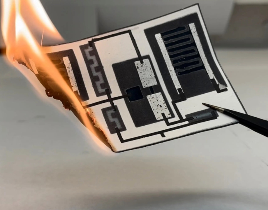
Seokheun “Sean” Choi, a professor of electrical and computer engineering at Binghamton University, has found a way to turn a huge chunk of the IoT into the Internet of Disposable Things by making those electronics out of paper. He’s created a paper circuit board that can be crumpled up and chucked in the compost or burned at the end of its life cycle. His paper, “Integrated Papertronic Techniques: Highly Customizable Resistor, Supercapacitor, and Transistor Circuitry on a Single Sheet of Paper,” appeared in Applied Materials & Interfaces this fall.
You Might Also Like: Recycling E-Waste Locally
Using paper as a substrate for electronics is not entirely new. Choi himself previously produced a chip using off-the-shelf electronics components on a paper backing. To make that work, the paper required lamination to reduce its porosity and roughness. But now Choi has taken advantage of those properties to embed the circuitry right into paper, making a completely biodegradable, truly papery, papertronic.
 Professor Seokheun “Sean” Choi has developed a process to create disposable circuit boards using paper and commercially available wax and inkjet printers. Photo: Binghamton University
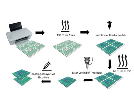
Choi’s technique is to first impregnate the paper with a pattern of wax, making those areas hydrophobic. The paper can absorb wax partially from one side, so that the circuit can be as three-dimensional as needed. Then, using inkjet printing, a conductive ink is printed on the paper in all the areas that have remained hydrophilic. Both the wax printer and the inkjet printer are commercially available.
With this method, Choi made a flexible, disposable, burnable, working circuit with capacitors and transistors, including n- and p-types.
Become A Member: How to Join ASME
The applications for such a device are many. They could track patients’ vital signs and connect them to their physicians; work with crop management and soil monitoring; help scientists monitor the oceans and other environments; monitor food spoilage in grocery stores; revolutionize shipment tracking; or provide cheap surveillance for the military.
“In the future, I believe that billions of disposable wireless devices will be deployed for special short-term missions,” Choi said. “Low cost and environmentally friendly devices are essential to providing disposable and biodegradable functionality.”
Of course, before paper circuitry gets deployed by the billions, there is work to be done. For one thing, Choi added graphene to the ink to increase its conductivity, but its biodegradability and toxicity when burned are not totally understood. To be safe, Choi is looking to replace the ink with one made of entirely biodegradable and nontoxic elements. He used filter paper for this first proof of concept because of its high porosity, but hopes to finesse the technique so that typical printer paper can be used.
Related Content: Turning E-Waste into an Opportunity
Despite these possible areas of improvement, the papertronic technology is close to ready for the many uses listed above. But could a paper chip actually replace a significant fraction of that 54 million metric tons of electronic waste?
“Resolution and integration must be improved significantly to reach conventional electronic capability,” Choi said. “But when you consider our target applications, maybe this is sufficient. If you want to use this technique for a one-time use application, maybe you don't need a super-duper electronic device.”
Regardless, Choi is up to the challenge of making papertronics as functional as the traditional stuff. “I try to convince people that papertronics will have different applications,” he said. “But people still want to compare the performance to that of conventional electronics. So, yeah, my target is to improve papertronics’ performance up to that in conventional electronics—but it’s challenging.”
Michael Abrams is a technology writer in Westfield, N.J.
Most electronics are thrown out at the end of their life cycle, but a disposable circuit board made of paper could help reduce the growing amount of electronic waste.

Freelance writer based in New Jersey
Related Content