Livermore Grows Advanced Manufacturing
Livermore Grows Advanced Manufacturing
Just as the assembly line ushered in the Industrial Revolution, new additive manufacturing (AM) techniques are creating new possibilities in a range of product manufacturing applications. The Advanced Manufacturing Lab at Lawrence Livermore National Laboratory, Livermore, CA, is at the forefront of this new era of on-demand fabrication of materials and parts that until now have been impossible to make with conventional technology.
LLNL teams are harnessing the power of advanced computing to refine an integrated end-to-end process that encompasses product design, material design, fabrication processes, and product certification. This new approach is accelerating manufacturing innovation to create products tailored to specific applications in military, medical, automotive, and consumer applications, at a pace never seen before.
As a U.S. Department of Energy lab, LLNL is dedicated to advancing science and technology that strengthens U.S. security. “Our modeling and new process development efforts are informed by the needs of the AM industry so that we can provide value to U.S. economic security,” says LLNL engineer Chris Spadaccini.
The Advanced Manufacturing Lab’s purpose is to develop new approaches to material and product creation and then integrating design, fabrication, and certification, in hopes of catalyzing the manufacturing world’s transformation.
Design and Visualization
The first step in this new process is design. By using high-performance computing (HPC), new product designs can be modeled virtually, and then optimized for specific uses without ever having to leave the digital realm. Computer modeling is hardly new to manufacturing, but AM techniques enable completely new designs and properties that require much more precise and intensive calculations. LLNL has been an HPC leader for decades. While most of the LLNL’s computing capabilities were developed to support national security missions, a synergistic offshoot has been the application of HPC for science and engineering applications such as AM design.
Creation
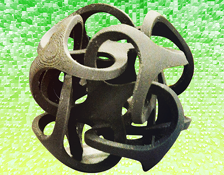
The second step is material development. Materials used in AM are called “feedstock.” New AM techniques under development at LLNL require advanced feedstock that is not commercially available so researchers must create their own in the laboratory. They also utilize chemical models and computing tools to synthesize materials digitally before compounding the real thing. The feedstock consumer, the additive manufacturing equipment itself — of which 3-D printers are the most widely used — get special treatment at LLNL’s AM Lab. Several types of known processes are used, but the abilities of standard equipment are greatly extended and enhanced.
For example, researchers are advancing the science (or art) of using light to “print” 3-D structures at the tens of microns scale. Using the process known as projection microstereolithography, UV light is flashed on various photosensitive liquids loaded with particles of ceramics or metals. Layer by layer, the 2-D images are cast and deposited on the previous layer, forming a 3-D shape. One example product of this process is an octet truss – an eight-sided skeleton that demonstrates high stiffness with very low weight. Layers of octets can be printed on top of each other, producing structures with incredible stiffness and strength at low weights, echoing the innovative architecture and designs of Alexander Graham Bell and Buckminster Fuller. Yet these structures are being printed by LLNL researchers and their collaborators at Massachusetts Institute of Technology using light to create micro-architectures for applications that will change industry — tens of microns at a time.
Certification
As with any manufactured part, certification testing is critical. LLNL is using its computational resources to accelerate this typically time consuming and expensive step. Product and material certification is important in many industries including automotive, aerospace, medical, and military. Materials must perform to their specifications; failure could be disastrous.
An LLNL initiative called Accelerated Certification of Additively Manufactured Metals seeks to develop predictive computer models for the lab’s AM-crafted materials and parts. To ensure the required level of precision and accuracy, the computer models are based on physics first principles and validated through physical experiments. LLNL is even pioneering approaches to sensing, monitoring, and control that can be used in real time during fabrication to ensure everything is happening according the specification. Controlling processes during fabrication, rather than afterward, can greatly reduce certification timelines and costs. Effectively, certification is being built-in to the process itself so products can be “born certified.”
Integration
Spadaccini says the models used to design the parts must account for both the properties of the feedstock and the capabilities of the fabrication process. Similarly, computational certification, supported by in-process sensing and control, must be based on the design criteria and specifications. The full-cycle approach can help address the unique needs of AM’s user base. “Integrating modeling and design, material synthesis, and manufacturing, we can better tailor our solutions for specific applications and needs,” he says. Having these capabilities available in a single lab, greatly enhances the power of each step’s individual innovation, advancing both the science and the industry-based applications.
Collaboration
To ensure their work doesn’t take place in a bubble, LLNL is collaborating with industry and local government AM initiatives. In the lab’s Bay Area backyard, the team participates in the i-Gate innovation partnership, a consortium of local governments, startups, venture capital firms, and researchers. Through i-Gate, a “FabLab” is being established to both energize the local “maker” community, as well as to demonstrate new techniques in AM for industry. In the state of California, the California Network for Manufacturing Innovation (CNMI) was recently formed to accelerate manufacturing innovation and technology adoption. Through the CNMI collaboration, partnerships of small- to large-sized companies will be able to leverage LLNL-developed intellectual property and AM techniques.
Michael MacRae is an independent writer.
Integrating modeling and design, material synthesis, and manufacturing, we can better tailor our solutions for specific applications and needs.Chris Spadaccini, Engineer, Lawrence Livermore National Laboratory
Related Content


