Inexpensive Semiconductors Reduce Costs of Solar Cells
Inexpensive Semiconductors Reduce Costs of Solar Cells
Despite a high level of interest in solar photovoltaic technology for producing sustainable energy, high material and manufacturing costs continue to hamper widespread adoption. However, a new technology developed by researchers at the U.S. Department of Energy's Lawrence Berkeley National Laboratory and the University of California Berkeley may change that. The technology, called "screening-engineered field-effect photovoltaics," or SFPV, enables low-cost, high efficiency solar cells to be made from virtually any semiconductor material.
The technique was unveiled in a research article published in the Journal of Nano Letters (July 2012) titled Screening-Engineered Field-Effect Solar Cells co-authored by Alex Zettl, William Regan, Steven Byrnes, Will Gannett, Onur Ergen, Oscar Vazquez-Mena and Feng Wang. Zettl holds joint appointments with Berkeley Lab's Materials Sciences Division and UC Berkeley's Physics Department where he directs the Center of Integrated Nanomechanical Systems.
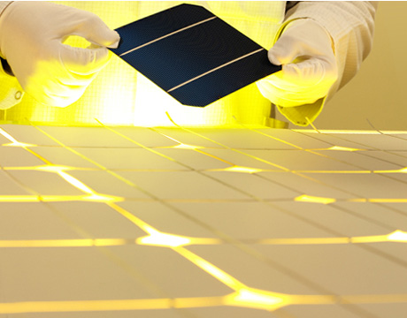
Until now, crystal silicon has been the material of choice for developing high-performance, highly reliable solar cells. Crystalline silicon is made by growing large cylindrical single crystals, called boules. The boules are sliced into thin wafers, from which photovoltaic devices are made. Slicing is an expensive and material-wasteful process.
Alternative Semiconductor Materials
There has been much recent research focused on developing alternative materials as a less expensive means of producing solar-grade silicon to lower the cost of photovoltaic power. SFPV technology enables the use of plentiful, relatively inexpensive, and non-toxic semiconductors, such as metal oxides, sulfides and phosphides, which were thought to be unsuitable for solar cells because of the difficulty in tailoring their properties by chemical means.
The most common photovoltaic cell structure consists of a semiconductor material into which a large-area diode, or p-n junction, has been formed. Electrical current is taken from the device through a grid contact structure on the front that allows the sunlight to enter the solar cell, a contact on the back that completes the circuit, and an antireflection coating that minimizes the amount of sunlight reflecting from the device. The fabrication of the p-n junction (an interface between regions with a deficit or an excess or electrons) is key to successful operation of the photovoltaic device.
The Zettl Research Group explains on their web site that the active material of a solar cell is chosen to be a semiconductor with an electronic bandgap near the peak of the solar spectrum. Excited electrons are pushed one way or the other by introducing some asymmetry into the semiconductor at the p-n junction. Despite an abundance of semiconductors with near-ideal bandgaps, only a few semiconductors can be made into high efficiency PV cells with high quality p-n junctions, either by chemical doping or by heterojunction formation. Several other promising PV materials are incompatible with chemical doping and form poor heterojunctions.
Chemical Doping of Semiconductor Materials
SFVP technology provides alternative means to effectively dope any semiconductor, including hard-to-chemically-dope materials, by applying an electric field through partially-screening electrode. Electric fields have long been used to modulate carrier concentration of semiconductors in the transistor industry, notably in metal-insulator-semiconductor field-effect transistors (MOSFETs). The top electrode of the cell is geometrically structuring to permit an electric field to pass through the electrode and locally "dope" the semiconductor, and the resulting cells are called SFPVs.
"Our technology can be thought of as combining a MOSFET and a standard solar cell. The challenge was adapting the field-effect gating to the solar cell architecture, and we overcame it by structuring our solar cell contacts in a way to let the electric field pass through the contacts and affect the semiconductor," says Will Regan, a grad student in the Zettl Research Group and lead author of the Screening-Engineered Field-Effect Solar Cells paper.
"The greatest engineering challenge was to understand fundamentally the geometry needed to make the partially screened electrodes work, tailored for each particular semiconductor," says Zettl. "Our theoretical model lets us input the optical/electronic parameters of the electrode material and the semiconductor in question, and then clearly defines the appropriate geometry. Without this, it would be endless trial and error."
Two distinct geometries of SFPV cells have been demonstrated — extremely narrow top contacts or "nanofingers" (type A) and extremely thin top contacts such as graphene (type B), which allow the electric field to bleed around or penetrate the contact. A novel self-gating strategy is employed to internally power the gate field, simplifying practical implementation of SFPV cells. Theoretical and experimental studies of this new method, using silicon as a proof of concept, indicate that this may be a compelling route to low-cost, high-efficiency photovoltaics and open the door to terawatt-scale deployment.
"A meaningful breakthrough in PV requires both low cost and high efficiency, as balance of system costs will offset any gains in low cost, low efficiency cells," says Regan. "Fortunately, our technology enables both. Our method is low cost, since we use mostly standard material deposition processes and can use just about any semiconducting material —anything from standard materials like silicon to abundant and cheap-to-process metal oxides, phosphides, and sulfides. Our gating strategy also lets us attain high efficiencies, since we can tune the best current heterojunctions into much better heterojunctions, with efficiencies closer to the Shockley-Queisser limit," he adds.
Tom Ricci is the owner of Ricci Communications.
A meaningful breakthrough in PV requires both low cost and high efficiency, as balance of system costs will offset any gains in low cost, low efficiency cells.Will Regan, a grad student in the Zettl Research Group
Related Content


