2-D Nanomaterials Revolutionizing Device Design
2-D Nanomaterials Revolutionizing Device Design
A new generation of nanoelectronic devices is emerging as a result of recent advances in research involving two-dimensional (2-D) nanomaterials.
The most widely studied 2-D nanomaterial is graphene, a single layer of carbon atoms only one molecule thick and packed in a hexagonal lattice. The material exhibits exceptional strength and possesses many other novel electrical and optical properties that have scientists buzzing since its first isolation in 2004. The electronic, thermal, and mechanical properties of graphene make it attractive for a variety of potential applications, including aerospace, automotive, electronics, energy storage, solar, oil service, and lubricant sectors.
However, graphene lacks one key property that has hampered development in electronic devices. Researchers have struggled to build electronic circuits out of graphene because the material lacks a bandgap, an important property that allows it to stop conducting or switch off, and is essential for many electronic applications.
Molybdenum disulfide (MoS2), another 2-D nanomaterial, is proving to be much better suited for designing electronic components. MoS2 has been used as an industrial lubricant for decades, but a Swiss research team uncovered its 2-D potential in 2011 for creating highly flexible thin-film transistors.
Improved Performance
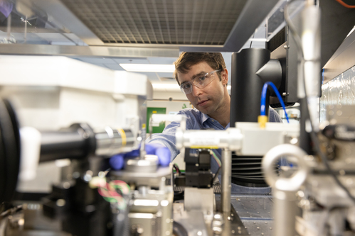
A report on the production of complex electronic circuits made from MoS2 was published in Nano Letters in August 2012. The paper, titled "Integrated Circuits Based on Bilayer MoS2 Transistors," was co-authored by Han Wang and Lili Yu, graduate students in the department of electrical engineering and computer science (EECS) at the Massachusetts Institute of Technology under the direction of Tomás Palacios, the Emmanuel E. Landsman Associate Professor of EECS.
According to Placios, MoS2 has a natural bandgap and overcomes the shortcomings of graphene while still exhibiting many of graphene's advantages for electronic and optoelectronic applications.
"The future of electronics is based on fabricating devices with these new, thin, 2-D materials," says Placios. "Graphene is only one atom thick while MoS2 is three atoms thick. The performance of many semiconductor devices, from transistors, to LEDs and sensors will significantly improve when we use these new 2-D materials."
Wang and Yu described a variety of basic electronic devices that were fabricated on the material: an inverter, which switches an input voltage to its opposite; a NAND gate, a basic logic element that can be combined to carry out almost any kind of logic operation; a memory device, one of the key components of all computational devices; and a more complex circuit called a ring oscillator, made up of 12 interconnected transistors, which can produce a precisely tuned wave output.
Potential Applications
Palacios envisions a wide array of potential applications for MoS2 and other 2-D materials. "At the beginning, it is most important that we don't try to compete with existing applications of high-tech electronics. The entry barrier is too high. For a completely new material and technology to be successful, we need to find completely new applications that cannot be done with existing semiconductors," he adds.
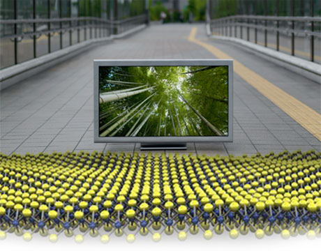
One of those applications envisioned by Palacios and his group is flexible and transparent electronic devices, such as displays embedded into a window of a house or office. "We want to enable ubiquitous electronics—we want electronic sensors in every building and we want clothes with electronic sensors, systems, and communications devices. We need a new type of material that can be fabricated in very large areas on a flexible substrate. You can't do this with conventional silicon," he says.
Another key application for MoS2 is chemical and biological sensors. According to Palacios, thanks to the electrical conductive properties of these thin 2-D materials, chemical sensors with extremely low noise performance and very high sensitivity could be fabricated. He also sees potential for light emitting devices such as LEDs and lasers.
Palacios predicts initial commercial applications of devices using these new materials could happen in 3-5 years. However, several challenges must still be solved.
"It is important that we find a way to fabricate very large areas of MoS2 at low cost," says Palacios. "Most of the results reported in the literature are based on small flakes of MoS2, just a few microns in length. We need to develop high-yield techniques to grow very large areas."
He adds that researchers need to understand how to reproducibly modify the charge density of the material in a controlled manner and further research on how light emission occurs in these materials.
"MoS2 is only the first material of a new family of 2-D semiconductors," says Palacios. "We need to perform more experimental and theoretical studies to see whether MoS2 is the best material or not. However, from what we know today, it looks very promising. We believe that the twenty-first century will be all about 2-D materials in the same way that the information revolution of the twentieth century was based on 3-D semiconductors, like silicon."
Tom Ricci is the owner of Ricci Communications.
The future of electronics is based on fabricating devices with these new, thin, 2-D materials.Tomás Palacios, Emmanuel E. Landsman Associate Professor, EECS, MIT
Related Content